Menu
Raman spectroscopy is a spectroscopic technique used to identify of biochemical substances or biomolecules. Raman spectroscopy relies on inelastic scattering, also known as Raman scattering, when a laser interacts with the molecules. The changes, or the shifts, of the energy of the laser photons can give information about the interacted molecules. This technique has been recently used to detect chemical or biomolecular substances, i.e., narcotic drugs, trace amount of materials, and emerging diseases.
However, most materials give out small Raman signals. In 1974, Fleischmann, et al. successfully developed a technique to amplify the Raman signals up to 6 times with highly roughened silver surfaces. The laser photons that interact with the free electrons in the metals will cause the resonance in these electron cloud. Such phenomenon, called the surface plasmon resonance, helps the energy transfers among the molecules within the proximity. This helps release the energy with higher Raman signals.
Generally, the Raman scattering can be observed when the conditions meet these 2 mechanisms. The first mechanism is the electromagnetic enhancement, which is caused by the stimulation of the surface plasmon resonance within the metal surfaces. The second is the chemical absorption of the molecules, and highly depends on the wavelength of the laser photons, the optical properties of the metals, and the surface structures of the substrates.
Until recently, there have been several processes to develop the substrates that help amplify the Raman signals and their efficiency. The surface-enhanced Raman scattering (SERS) substrates have been a subject of interests among scientists. Theoretically, the SERS substrates can be developed from gold, silver, copper, or other noble metals, and have been widely used in the detections of the biomolecules and chemical molecules.
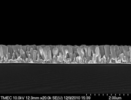
The NECTEC SERS Chips (Fig. 1) has been developed with our advanced thin-film depositions with the sputtering system by Optical Thin-Film Technology Laboratory (OTL), National Electronics and Computer Technology Center (NECTEC). We have successfully fabricated thin-film-based nanostructures of silver metals (Fig. 2) with unique properties to highly enhance the Raman signals. Our SERS Chips, which come in full packages at a cost-effective price, can yield up to 100 times the Raman signals when compared with those from the commercially available products. The NECTEC SERS Chips can be readily used for trace detections of the trace amount of many substances, which are no longer detectable from conventional Raman spectroscopic technique.
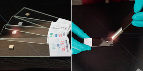
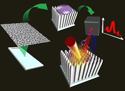
To use the NECTEC SERS Chips, operators can simply swab or wipe an area suspected to be exposed to chemical substances of interest, even though imperceptible to the naked eyes. The swabbed sampling can be quickly dissolved in a solvent. A small volume (2-3 microliters are sufficient) is then dropped on the surface of the NECTEC SERS chips. And now the operators can go right to the characterizations or analyses with any Raman spectroscopes (Fig. 3). The NECTEC SERS Chips are fully compatible with all research-grade, portable, or even handheld Raman spectrometers available in the markets.
Currently, the NECTEC SERS Chips are successfully utilized in a wide ranges of applications, for examples, trace detections in agricultural products (pesticides), forensic investigations (narcotic drugs, explosive substances, pen inks), and medical studies (biomolecules). OTL has published academic journals and filed several patent applications with complete protections of our inventions.
Team:

- Optical Thin-Film Technology Laboratory (OTL)
- National Electronics and Computer Technology Center (NECTEC)
- e-mail: otl[at]nectec.or.th
- https://www.facebook.com/OTL.NECTEC/
More information:
- Business Development and Technology Transfer (BTT)
- National Electronics and Computer Technology Center (NECTEC).
- Tel: +662 564 6900 ext2346, 2351-2354, 2357, 2382, 2383, 2399
- e-mail: business[at]nectec.or.th