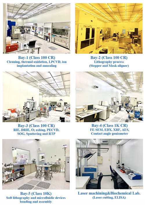
1. Advance Lithography Process
- Photomask design and fabrication
- Thin film deposition (SiO2, Si3N4, Poly-Si, a-Si, TEOS, SOG, Al, Ti, TiN, etc.)
- Chemical etching and plasma etching (RIE and Deep-RIE)
- Silicon mold and intermediate polymer mold fabrication
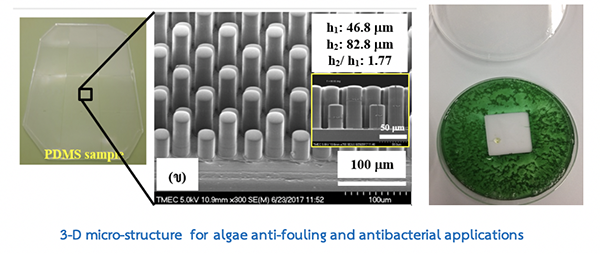
- Soft lithography process (Polymer micro-structure fabrication)
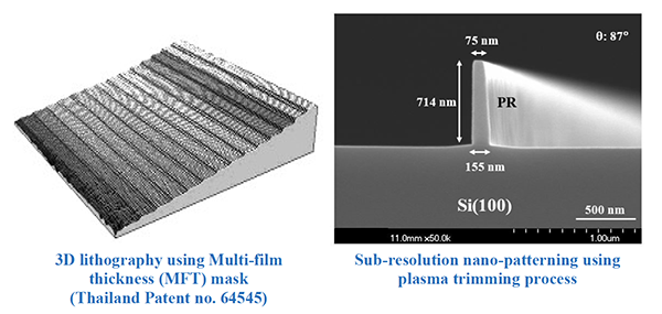
- Sub-resolution patterning (Sidewall Image Transfer (SIT) technology, Photoresist trimming process, and multiple-patterning process)
- 3-D patterning by greyscale lithography and Multi-film thickness mask (MFT-mask)
2. Surface Innovation Technology Platform
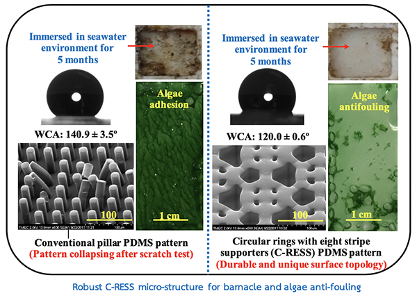
- Composite materials with low-surface energy
- Slippery Liquid-Infused Porous Surfaces (SLIPS)
- Frame treatment process (Nano-texturing)
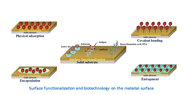
- Surface functionalization
- Molecular analysis
- Superhydrophobic and superoleophobic surface
- Anti-bacterial and anti-fouling technologies
- Large-area patterning (R2R and R2P) (collaboration with international partners)
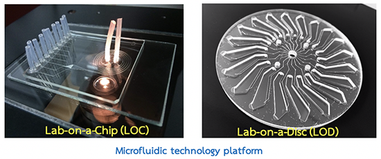
3. Microfluidic technology platform
- Microfluidic devices [Lab-on-Chip (LOC), Lab-on-Disc (LOD), Organ-on-Chip (OOC)]
- Micro-droplet devices (cell sorting/cell trapping/cell culturing)
- Plasma bonding and laser cutting
- High-throughput injection molding (collaboration with international partners)
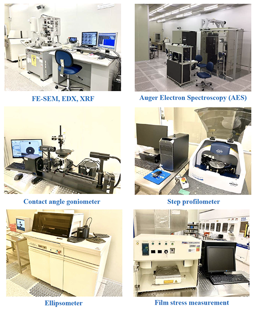
4. Advanced material characterizations and surface analysis
- Field-emission Scanning Electron Microscope (FE-SEM) (with Energy Dispersive X-ray Spectroscopy (EDX) and X-ray Fluorescence (XRF))
- Auger Electron Spectroscopy (AES)
- Contact angle goniometer
- Spectrophotometer
- Ellipsometer
- Film stress measurement
- Step profilometer
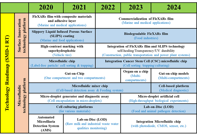
Surface innovation technology platform
1. FleXARs Technology
Large-area flexible polymers with antifouling robust micro-structure for marine, medical, and transportation applications (FleXARs project –an everything-free surface).
2. Slippery Liquid-Infused Porous Surface (SLIPS project)
To produce a large-area antifouling surface for marine & medical applications and public transportation system.
3. High-contrast Marking Vehicle Tire
Ultra-low light reflectivity micro-structure for vehicle and optical devices

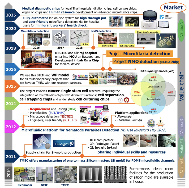
Microfluidic Technology Platform
1. Microfluidic Technology Platform
Microfluidic technology platform for cell sorting/cell trapping/cell culturing of cancer stem cell (CSC) and development of micro-droplet generator and diagnostic assay for rapid and high-throughput biological experiments
2. Lab-on-a-Disc (LOD)
Technology platforms of lab-on-a-disc (LOD) for semi-automated Microfilaria detection system (AMS) and LOD for raw milk quality monitoring system
3. Gut-on-a-Chip (GOC)
Technology platform of Gut-on-a-chip based on microfluidics technology for toxicology and pharmacokinetic study of food and pharmaceutical industries and others